


Blind vs Buried vs Micro Vias: A Complete Guide to PCB Via Technologies
 25 Sep 2026
By Jack Liu
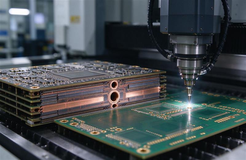
Compact electronics are squeezing more function into less board area, leaving designers less room for routing. Fine-pitch BGAs, dense modules, high-speed interfaces, and growing layer counts quickly turn a conventional through-hole via into a bottleneck. Blind vias, buried vias, and microvias solve this by connecting selected PCB layers without consuming the routing space a standard via takes up on every layer. For OEM and ODM buyers, choosing an advanced via structure is never purely an engineering call — it directly influences layer count, fabrication process, yield, reliability, lead time, and total cost. This guide explains how each via type works and what to prepare before requesting a quotation.
________________________________________
________________________________________
What Is a PCB Via?
A via is a plated conductive hole that electrically connects copper features on different PCB layers. Unlike a plated through-hole used to mount a component lead, a standard via is primarily an interconnection structure. A conventional through-hole via passes through the entire board — economical, but it occupies routing space on every layer it crosses. Blind and buried vias limit the via to specific layers; microvias go further with very small, shallow interconnections, typically used in HDI boards.
One point matters for procurement: “blind” and “buried” describe where a via connects inside the board, while “microvia” defines a specific small via structure by its physical dimensions. The two labels are not interchangeable — a microvia can therefore also be a blind via.
________________________________________
What Is a Blind Via?
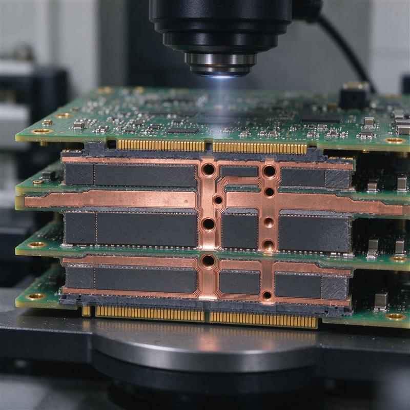
A blind via starts on an outer PCB surface and connects to one or more internal layers without passing through the whole board. On an 8-layer PCB, a blind via might connect Layer 1 to Layer 2 or Layer 8 to Layer 6. Blind vias are formed by laser drilling or controlled-depth mechanical drilling, depending on layer span and hole size.
Procurement tip: When requesting a quotation, specify the exact blind-via layer pairs in your stack-up documentation. Saying only “blind vias required” is not enough — the factory needs to know which layers connect.
________________________________________
Why Use Blind Vias?
The main benefit is routing efficiency. A through-hole via can block routing channels on multiple layers, while a blind via occupies only the layers it actually connects — especially useful around fine-pitch BGA packages. Blind vias can also remove unnecessary via stubs, which helps certain high-speed designs where signal integrity matters.
________________________________________
________________________________________
What Is a Buried Via?
A buried via connects internal PCB layers only and never reaches either outer surface. For example, Layer 3 to Layer 4 can be routed as a buried connection inside a multilayer board. Because the via is fully enclosed after lamination, it cannot be visually inspected from the outside. Buried vias are created during intermediate fabrication stages, before the complete multilayer structure is laminated together.
________________________________________
When Are Buried Vias Useful?
Buried vias add routing flexibility without consuming valuable outer-layer space. They help when internal routing density is very high or fine-pitch parts need maximum surface routing area. The trade-off is process cost: buried vias usually need additional lamination, drilling, plating, and inspection steps. For many cost-sensitive products, a conventional through-hole structure is preferable when it can still meet the routing requirements.
________________________________________
What Is a Microvia?
A microvia is a very small via structure widely used in HDI PCBs. Under IPC terminology, a microvia is a blind structure with a maximum aspect ratio of 1:1 and a total length of no more than 0.25 mm from the capture land to the target land. Microvias are typically produced by laser drilling rather than mechanical drilling.
Their small size lets designers place interconnections where a conventional drilled via would simply be too large — ideal for fine-pitch BGA packages, smart home products, and high-density industrial control boards.

________________________________________
Stacked and Staggered Microvias
When a design must connect through more than one HDI layer, microvias can be arranged in different structures. Staggered microvias are offset from one layer to another, creating a stepped routing path. Stacked microvias sit directly above one another, delivering excellent routing density but requiring more demanding fabrication and copper-filling processes.
________________________________________
Blind vs Buried vs Microvias: What Is the Difference?
|
Via Type
|
Connection
|
Typical Manufacturing
|
Main Benefit
|
Cost/Complexity
|
|---|---|---|---|---|
|
Through-hole
|
Outer layer through entire board
|
Mechanical drilling
|
Simple and economical
|
Low
|
|
Blind via
|
Outer layer to selected inner layer
|
Laser or mechanical drilling
|
Saves routing space
|
Medium
|
|
Buried via
|
Inner layer to inner layer
|
Mechanical/laser + sequential fabrication
|
Preserves outer-layer space
|
High
|
|
Microvia
|
Very small, shallow interconnection
|
Usually laser drilling
|
Maximum routing density
|
High
|
________________________________________
How Via Technology Affects PCB Cost
Advanced vias do not automatically make a board better for every application. Cost can rise because the board may need additional lamination cycles, laser drilling, via filling, extra copper plating, and more detailed inspection. A simple industrial controller, for example, may gain nothing from an HDI structure if through-hole vias plus standard blind vias already satisfy the routing. Conversely, removing HDI from a compact BGA design may force the board larger or push up the layer count, making the final product more expensive overall.
Procurement tip: Compare the total PCB solution — not just the quoted price of an individual via technology. A slightly higher unit price can still deliver the lowest total cost.
________________________________________
How to Choose the Right Via Technology
Start with the product requirements, not the manufacturer's preferred process. Fine-pitch BGAs and high-pin-count devices are the most common reasons to consider microvias — if the BGA pitch is relatively large and conventional vias can complete the routing, an HDI structure may be unnecessary. When board dimensions are tightly restricted, blind and microvia structures create extra routing channels without adding board area. High-speed interfaces may benefit from shorter electrical paths and reduced via stubs, but via selection must be evaluated together with impedance control, stack-up, and material selection. For medical, industrial, automotive, and other demanding applications, reliability comes before complex structures such as stacked microvias. For OEM buyers, a DFM review before mass production is essential.
________________________________________
What Should Buyers Tell a PCB Manufacturer?
When requesting a quotation for a board with blind, buried, or microvias, provide as much fabrication information as possible. At minimum, the manufacturer should receive:
- PCB layer count
- Finished board thickness
- Stack-up information
- Via type and layer pairs
- Finished hole sizes
- Copper thickness
- Microvia dimensions, if applicable
- Whether vias require filling
- BGA pitch and component information
- Controlled impedance requirements
- PCB quantity and expected annual volume
A complete fabrication package lets the supplier evaluate manufacturability instead of estimating from incomplete information.
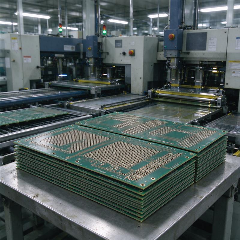
Key procurement tip: Ask the PCB manufacturer to confirm the proposed via structure during engineering review before placing the mass-production order. A design that is theoretically possible may still need process adjustments for stable production yield.
________________________________________
Common FAQ About PCB Vias
Q1: Are blind vias and microvias the same?
No. A blind via connects an outer layer to an internal layer without passing through the entire board. A microvia is a small, shallow via defined by specific dimensional and aspect-ratio criteria, commonly a type of blind structure used in HDI PCBs.
Q2: Are buried vias more expensive than through-hole vias?
Generally yes. Buried vias require additional fabrication steps because they must be formed and plated before the complete multilayer structure is assembled. Actual cost depends on stack-up and quantities.
Q3: Are microvias always laser drilled?
Microvias are commonly formed by laser drilling in modern HDI manufacturing, though the IPC definition focuses on the resulting structure, not the drilling machine used.
Q4: Do microvias need to be filled?
Not every microvia needs the same treatment. Filling becomes important for certain stacked structures and via-in-pad applications, and should be decided from the design requirements.
Q5: Which via is best for a PCB?
There is no universal best via. The right choice depends on PCB size, component pitch, layer count, electrical requirements, reliability targets, production volume, and cost — use the simplest structure that reliably meets the requirements.
________________________________________
Final Thoughts
Blind vias, buried vias, and microvias give designers powerful tools to increase routing density and support increasingly compact products — particularly HDI boards, fine-pitch BGA packages, and space-constrained applications. For OEM and ODM buyers, advanced via technology is both a design decision and a manufacturing decision: the right structure can shrink board size and improve routing flexibility, while an unnecessarily complex one can raise cost and manufacturing risk.
Involve a capable PCB and PCBA supplier early in the design process to balance performance, manufacturability, reliability, and total cost. Planning a new PCB project or ready to compare via options for your next design? Contact our engineering team for a free DFM review and a customized quotation.
Latest Post
-
How to Improve Signal Integrity in High-Speed PCB Design?
19 Oct 2026 -
What Is PCBA Functional Testing? A Complete Guide
11 Sep 2026 -
How to Avoid Common PCB Assembly Defects: A Complete Guide
17 Aug 2026 -
SMT vs Through-Hole Assembly: Which One Should You Choose?
23 Jun 2026 -

What is DFM in PCB Design? A Complete Guide for Exporters & Startups
20 May 2026 -

How to Reduce PCB Manufacturing Cost: 10 Actionable Tips for 2026
09 May 2026