


How to Improve Signal Integrity in High-Speed PCB Design?
 19 Oct 2026
By Jack Liu
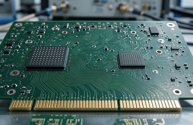
High-speed multilayer PCB with parallel differential pairs, BGA packages and an impedance test coupon at the board edge
Data rates on today's boards have left 100 MHz layout habits far behind. DDR4, USB 3.0, HDMI 2.0 and gigabit Ethernet are routine on industrial controllers, smart-home gateways and medical devices — and at those speeds a board that passes schematic review can still fail in the field. For OEM and ODM buyers, signal integrity shows up as field returns, failed EMC certification and repeated design spins before volume production. This guide covers the causes, the fixes, and what to verify with your manufacturing partner.
________________________________________
What Signal Integrity Means for a Finished Product
Signal integrity is the ability of a signal to reach the receiver without distortion. On a high-speed board the signal is no longer a clean 0 or 1 — it behaves as a high-frequency wave shaped by trace geometry, dielectric properties and nearby copper. When it degrades, the result is bit errors, intermittent resets, failed EMI tests and shrinking timing margins.
Mixed-technology boards need particular care. Designs pairing fine-pitch SMT parts with rugged power or mechanical connectors must protect high-speed nets from layout through assembly, whether the build runs on high-density SMT PCBA manufacturing lines or needs selective through-hole PCB assembly.
________________________________________
Where High-Speed Designs Usually Fail
Four root causes explain most failures in buyer projects.
Impedance mismatch. Every high-speed trace has a characteristic impedance — typically 50 ohm single-ended, 90 or 100 ohm differential. When trace width, dielectric thickness or the reference plane changes abruptly, part of the signal reflects back as ringing and overshoot.
Crosstalk. Parallel traces running over a long distance with tight spacing couple energy into each other, a common issue in dense DDR and bus routing.
Loss and attenuation. The laminate itself absorbs energy at high frequency. Low-cost FR-4 can cause significant insertion loss above 5 Gbps, closing the eye diagram at the receiver.
Return path discontinuity. High-frequency current returns directly beneath its signal trace. A plane split, a missing ground via or a crossing over a void forces that current into a long loop, creating noise and EMI.
|
Issue |
What Causes It |
What You Observe |
First Fix |
|
Impedance mismatch |
Abrupt change in trace width, dielectric height or reference plane |
Ringing, overshoot, reflections |
Fix the stack-up, control impedance |
|
Crosstalk |
Long parallel runs with tight spacing |
Jitter, false switching on buses |
Widen spacing, keep pairs coupled |
|
Loss and attenuation |
High-loss laminate absorbing energy above 5 Gbps |
Closed eye at the receiver |
Move to low-loss material |
|
Return path discontinuity |
Plane splits, missing ground vias, connector breaks |
EMI, noise margin loss |
Stitch grounds, never cross a void |
________________________________________
Seven Practical Strategies to Improve Signal Integrity
Start With the Stack-up and Material Choice
Above 1 Gbps we recommend at least a 6-layer build with dedicated ground planes adjacent to the high-speed signal layers, keeping the return path continuous and low in impedance.
Standard FR-4 stays workable for most consumer and industrial products up to roughly 3–4 Gbps. For 10 Gbps and above — medical imaging, high-end smart-home gateways — low-loss laminates such as Isola FR408HR or Panasonic Megtron 6 offer lower Dk and Df.
Define and Verify Controlled Impedance
Impedance must be specified, not assumed. Agree controlled-impedance traces and tolerance with your manufacturer — typically ±10%, tightening to ±5% for DDR and PCIe Gen3 and above. That demands tight control of trace width, copper thickness and dielectric height. A capable partner keeps impedance coupons on every panel and ships TDR reports with the boards.
|
Procurement tip: Ask directly whether impedance test reports are provided for every production lot. Suppliers who test per panel and document the data are usually the same ones who hold tolerances during volume ramp. |
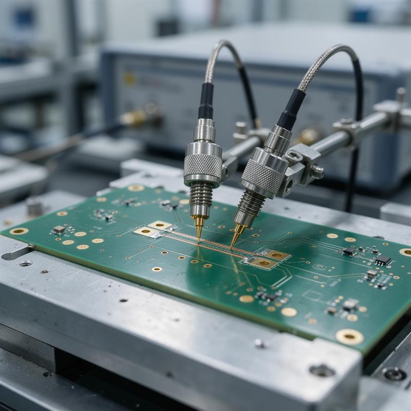
RF probes contacting an impedance test coupon on a high-frequency PCB panel before TDR measurement
Apply Real Routing Rules to High-Speed Nets
Layout is where margin quietly disappears. Keep differential pair traces equal in length within about 5 mils, hold constant spacing and route them symmetrically. Avoid unnecessary vias. Use serpentine routing sparingly and keep the amplitude small; match DDR byte groups within the group rather than across the whole bus. Apply the 3W rule for spacing, and use 5W or ground guard traces on critical clocks.
Protect the Return Path
Never route a high-speed signal across a split in its reference plane. If a crossing cannot be avoided, place stitching capacitors near the crossing point to give the return current a high-frequency path. Add ground stitching vias wherever a signal changes layers, because the return current must change layers too. This matters most in mixed builds, where through-hole connectors can interrupt ground planes — plan connector placement early.
Reduce Via Discontinuities
Vias are impedance discontinuities, so use fewer and better ones. Smaller drills, removal of unused inner-layer pads and back-drilling on thick boards all shorten the stub. A via stub acts like an open antenna and resonates at frequencies that matter in high-speed links. For BGA breakouts, filled and capped via-in-pad keeps the path short.
Pair Termination With Decoupling
Termination prevents reflections: source series termination for point-to-point nets, parallel or Thevenin termination for multi-drop buses, with resistors placed close to the source or load. Decoupling supports power integrity, which cannot be separated from signal integrity. Place 0.1 µF and 0.01 µF capacitors close to high-speed IC power pins and connect them to the power plane with short, wide traces.
Simulate Before You Build
Rules alone will not predict margin. SI simulation can produce eye diagrams, crosstalk estimates and impedance profiles before a single panel is fabricated. If you manage an external design team, require a pre-layout SI report on stack-up and routing strategy, plus post-layout verification of the critical nets. That small investment prevents a costly respin.

Oscilloscope screen showing a measured eye diagram for a high-speed serial link
________________________________________
Holding Signal Integrity Through Manufacturing and Assembly
A clean design can still be undone on the production floor. Solder paste printing and reflow profile control determine the quality of high-speed connector and BGA joints, and excessive voiding under a BGA ground pad raises ground inductance. On boards combining SMT with through-hole assembly, wave soldering temperature and fixture design must be controlled to prevent warpage that changes dielectric thickness.
A professional partner manages these through AOI and X-ray inspection of BGA and QFN joints, impedance testing on every production panel, strict material traceability, and assembly to IPC-A-610 Class 2 or Class 3 for industrial and medical electronics.

Automated optical inspection scanning a panel of assembled high-speed boards on an SMT line
________________________________________
Supplier Qualification Checklist for High-Speed Projects
Four questions for supplier qualification.
• Engineering capability: Can the team review my stack-up and give DFM and DFT feedback focused on high-speed signals?
• Material and process control: Are low-loss laminates available, and is the same material brand guaranteed for volume production?
• Testing and data: Are impedance coupons, TDR reports and SI-related data supplied with each shipment?
• Assembly experience: What is the track record with DDR4, USB 3.0 and PCIe across SMT and through-hole projects?
Suppliers who answer with data and case studies are more likely to hold performance at volume.
|
Key procurement tip: Share your target impedance, data rate and certification plan at the quotation stage. A supplier who sees those constraints before fabrication can flag stack-up risks while changes are still free. |
________________________________________
FAQ
Q1: What is the most common cause of signal integrity problems?
Return path discontinuity — usually a plane split or a missing ground stitching via near a layer transition. It is easy to miss in layout review and expensive to discover after certification testing.
Q2: At what data rate do I need controlled impedance?
Any interface above roughly 100 MHz with fast edge rates benefits from it. Treat 1 Gbps and above as mandatory, with tighter tolerance for DDR and PCIe Gen3 or newer.
Q3: Is standard FR-4 good enough for high-speed designs?
For many consumer and industrial products up to about 3–4 Gbps, yes. Above that, insertion loss dominates and low-loss laminates pay for themselves by keeping the eye open.
Q4: Do blind and buried vias help signal integrity?
Yes. Limiting a via to the layers it connects removes stubs that would otherwise resonate, which is why HDI stack-ups with microvias and back-drilling are common on dense high-speed designs.
________________________________________
Final Thoughts
Improving signal integrity is rarely about adding complexity. It comes down to disciplined stack-up design, controlled routing, a continuous return path, and a manufacturing partner who understands high-frequency behaviour. For small and medium OEM buyers, the most cost-effective move is to involve that partner early — share your speed targets, impedance requirements and application scenario while the quotation is still being prepared.
If your next product involves high-speed interfaces, start with a signal integrity review before layout is frozen. Contact our engineering team for a free stack-up and DFM review, or request a quotation for custom PCB and PCBA assembly.
-
Blind vs Buried vs Micro Vias: A Complete Guide to PCB Via Technologies
25 Sep 2026 -
What Is PCBA Functional Testing? A Complete Guide
11 Sep 2026 -
How to Avoid Common PCB Assembly Defects: A Complete Guide
17 Aug 2026 -
SMT vs Through-Hole Assembly: Which One Should You Choose?
23 Jun 2026 -

What is DFM in PCB Design? A Complete Guide for Exporters & Startups
20 May 2026 -

How to Reduce PCB Manufacturing Cost: 10 Actionable Tips for 2026
09 May 2026